
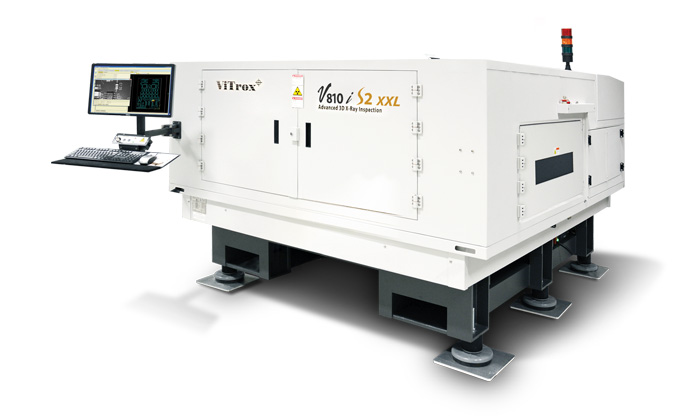
ViTrox V810i
Designed for various sizes of PCB assemblies to increase production efficiency and cost savings for Electronic Manufacturing Services (EMS), Original Equipment Manufacturers (OEMs), Original Design Manufacturers (ODMs), and etc.
- 为提高生产效率,降低EMS、OEM、ODM电子制造成本而设计的3D在线X光检测设备
|
Allowable Panel Characteristics ** |
V810i S2EX |
V810i S2 XXL |
V810i S2 XLT |
|
Maximum panel size |
482 mm x 610 mm (19"x24") |
660 mm x 965 mm (26"x38") |
660 mm x 965 mm (26"x38") |
|
Minimum panel size |
76 mm x 76 mm (3" x 3" ) |
76 mm x 76 mm (3" x 3" ) |
76 mm x 76 mm (3" x 3" ) |
|
Maximum panel inspectable area |
474 mm x 610 mm (18.7"x24") |
654 mm x 965 mm (25.75"x38") |
654 mm x 965 mm (25.75"x38") |
|
Maximum panel thickness |
7 mm (276 mils) |
12.7 mm (500 mils) |
12.7 mm (500 mils) |
|
Minimum panel thickness |
0.5 mm (20 mils) |
0.5 mm (20 mils) |
0.5 mm (20 mils) |
|
Panel warp |
Downside < 3.3 mm; Upside < 1.5 mm |
Downside < 3.3 mm; Upside < 3.3 mm |
Downside < 3.3 mm; Upside < 3.3 mm |
|
Maximum panel weight |
4.5kg |
15kg |
15kg |
|
Board top clearance |
50 mm @ 23 µm resolution |
25 mm @ 19 µm resolution |
50 mm @ 19 µm resolution |
|
Board bottom clearance |
70 mm |
80 mm |
80 mm |
|
Panel edge clearance |
3 mm |
3 mm |
3 mm |
|
Panel width tolerance |
±0.7 mm |
±0.7 mm |
±0.7 mm |
|
System resolution |
23 µm/19 µm#, 11 µm, 10.5µm, 6µm# |
19 µm/13 µm |
19 µm/15 µm /11 µm/10µm/7.5 µm |
|
100% Press-fit testability |
Yes (With PSP2 feature) |
Yes (With PSP2 feature) |
Yes (With PSP2 feature) |
|
Maximum acceptable panel temperatures |
40 Deg C |
40 Deg C |
40 Deg C |
|
Power and Environmental |
|||
|
System footprint (Width X Depth X Height) |
1566 mm x 2145 mm x 1972 mm |
2240 mm x 2460 mm x 1980 mm |
2240 mm x 2460 mm x 1980 mm |
|
Weight |
~3500 kg |
~5500 kg |
~6000 kg |
|
*Note: |
|||
Advanced Technologies
- Proprietary Hybrid Auto Focus Technology
- Solder Profile Characteristic
- Dynamic Range Optimization (DRO)
Image Quality
- Image Enhancement
- 3D CT Image
- Point Spread Function (PSF)
Improve Test Coverage
- Phase Shift Profilometry (PSP 2)
- New Voiding Algorithm
- PTH Detection
- BGA
- Broken Pin Algorithm
Ease of Buy Off
- ViTrox Verification Tool Solution (VVTS) Repair Station
- Auto Reject
- Good Image Comparison
- Diagnostic Image
- 2.5D PTH & BGA Angle View
Speed Improvement
- Real Time Predictive Slice Height (PSH)
- SUMO
- SPAM with Variable Scan Path
- 64 bits Image Reconstruction Processor (IRP)